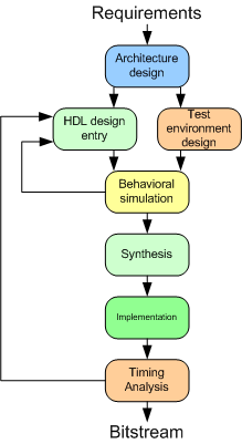
FPGA engineering process usually involves the following stages:

- Architecture design. This stage involves analysis of the project requirements, problem decomposition and functional simulation (if applicable). The output of this stage is a document which describes the future device architecture, structural blocks, their functions and interfaces.
- HDL design entry. The device is described in a formal hardware description language (HDL). The most common HDLs are VHDL and Verilog.
- Test environment design. This stage involves writing of test environments and behavioral models (when applicable). They are later used to ensure that the HDL description of a device is correct.
- Behavioral simulation. This is an important stage that checks HDL correctness by comparing outputs of the HDL model and the behavioral model (being put in the same conditions).
- Synthesis. This stage involves conversion of an HDL description to a so-called netlist which is basically a formally written digital circuit schematic. Synthesis is performed by a special software called synthesizer. For an HDL code that is correctly written and simulated, synthesis shouldn't be any problem. However, synthesis can reveal some problems and potential errors that can't be found using behavioral simulation, so, an FPGA engineer should pay attention to warnings produced by the synthesizer.
- Implementation. A synthesizer-generated netlist is mapped onto particular device's internal structure. The main phase of the implementation stage is place and route or layout, which allocates FPGA resources (such as logic cells and connection wires). Then these configuration data are written to a special file by a program called bitstream generator.
- Timing analysis. During the timing analysis special software checks whether the implemented design satisfies timing constraints (such as clock frequency) specified by the user.