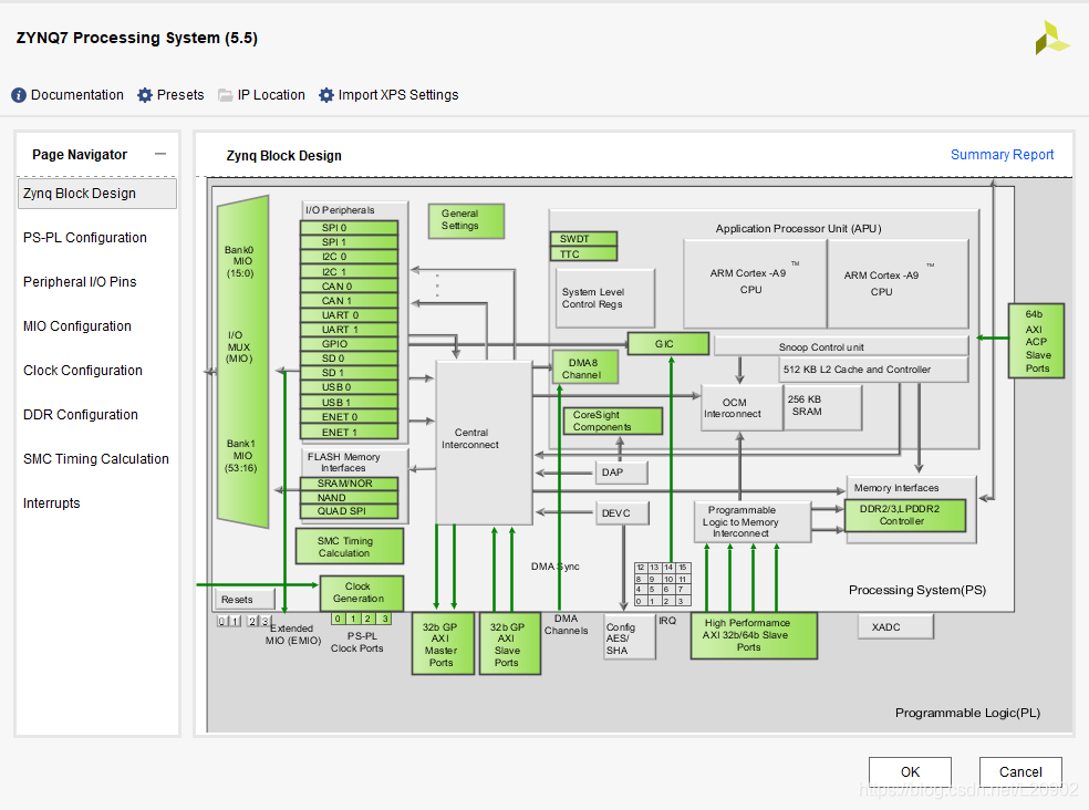
The Zynq-7000 SoC solution reduces the complexity of an embedded design by offering an Arm Cortex-A9 dual core as an embedded block, along with programmable logic on a single SoC.
For Zynq devices, the Vivado IP integrator captures information about the processing system (PS) and peripherals, including configuration settings, register memory-map, and associated logic in the programming logic (PL) fabric. You can then generate a bitstream for PL initialization.
The following figure illustrates the tools flow for the embedded hardware of a Zynq device:

完成一个设计,可按照以下步骤执行To complete an embedded processor design, you typically go through the following steps:
1. Create a new Vivado Design Suite project.
2. Create a block design in the IP integrator tool and instantiate a Xilinx processor, along with any other Xilinx IP or your custom IP.
3. Generate Output Products of the IP in the block design with the correct synthesis mode option.
4. Create a top-level wrapper and instantiate the block design into a top-level RTL design.
5. Run the top-level design through synthesis and implementation, and then export the hardware to SDK.
6. Create your software application. In SDK, associate the Executable Linkable File (ELF) file with the hardware design.
7. Use the Xilinx updatemem utility to merge the ELF and Memory Map Information (MMI) for the block Rams with the hardware device bitstream.
8. Program into the target board.
接下来是整理的教程,关于:(官方文档是全英的 懒得翻译了)
Using a Zynq-7000 Processor in an Embedded Design
1.create block design
2.add IP from the IP catalog
3. search for and select the ZYNQ7 Processing System

4. Double-click the processing system graphic to invoke the Re-customize IP process,which displays the Re-customize IP for the ZYNQ7 Processing System dialog box.The green colored blocks in the ZYNQ7 processing system (PS) are configurable items.You can click a green block to open the coordinating configuration option.
