The most common switching-power topology is a buck converter, which efficiently transforms high voltages to low voltages.

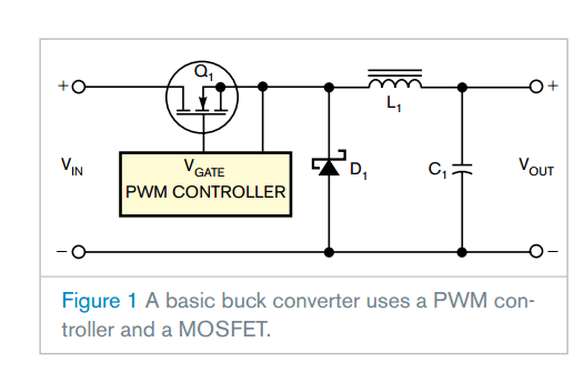
Figure 1 shows a typical buck converter in which the N-channel MOSFET, Q1, needs a floating-gate drive signal. The floating-gate drive is part of the PWM (pulse-width-modulation) controller IC. Q1 can be either N or P channel, depending on the controller’s design. Unfortunately, the IC’s voltage rating must be as high as the input voltage, which places a limit on the maximum voltage it can process.

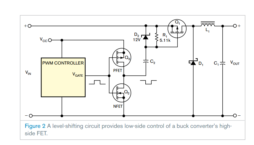
The circuit in Figure 2 uses a simple voltage-level shifter that lets a buck converter control a pass transistor with a low-side IC that has a ground-referenced gate drive. Because the level-shifting circuit in the PWM IC does not have to tolerate high voltages, you can implement a converter with an arbitrarily high input voltage.
PWM ICs with low-side gate drivers can power N-channel MOSFETs that are on when they have a positive gate-to-source voltage. The circuit in Figure 2 uses a P-channel device as the high-side MOSFET; it’s on when its gate-to-source voltage is negative. Therefore, you must invert the control signal from the PWM controller. A MOSFET totem-pole configuration comprising Q2 and Q3 will work, although you can also use an inverting-gate driver.
Capacitor C2 performs the level-shifting. It must have a value large enough to maintain its charge at the switching frequency but small enough for its voltage to follow variations in the input voltage. Resistor R1 and P-channel MOSFET Q3 charge C2 to a voltage of VC=VIN–VCC, where VC is C2’s voltage, VIN is the input voltage, and VCC is the supply voltage of the Q2 and Q3 totem-pole configuration and the PWM IC. The supply voltage must be less than zener diode D2’s breakdown voltage. Otherwise, current will flow through D2 and C2 whenever Q2 is on, which lowers efficiency. D2limits C2’s voltage to the value in the above equation. When Q3 is on, D2 becomes forward-biased if the voltage attempts to increase. This circuit applies a 0V voltage between Q1’s gate and source when Q3 is on, and it applies –VCC when Q2 is on.
Resistor R1 also ensures that Q1’s gate-to-source capacitance discharges, which keeps Q1 off when the totem pole’s output voltage is high. Diode D2 limits Q1’s gate-to-source voltage to 12V regardless of the circuit’s input voltage. Capacitor C2 is transparent to Q1’s gate-drive pulse, so the circuit’s gate-driving capability is just as good as that of the totem-pole circuit itself. The level shifting, therefore, imposes no limitation on the size of the MOSFET that the circuit can drive.
Figure 3 shows a practical buck converter employing this scheme.

The converter’s input voltage is 18 to 45V, and its output voltage is 12V at a 1.5A output current. The converter uses National Semiconductor’s LM5020-1 flyback/boost/forward/SEPIC (single-ended-primary-inductance-converter) PWM-controller IC.
The figure retains the component designators from the previous figures but adds functions such as input-voltage filtering in C9; input-undervoltage lockout in R2 and R7; soft-start capability in C3; switching-frequency-setting ability in 12.7-kΩ R3 for 500 kHz; feedback compensation in C7, C8, and R6; and output-voltage setting in R9 and R10.
The LM5020-1 provides current-mode control, but, in this circuit, it implements voltage-mode control. An internal sawtooth-current source with a peak value of 50 μA, which adds slope compensation to a current signal, serves as a voltage ramp. This current flows through 5.11-kΩ resistor R4 and an internal 2-kΩ resistor to generate a ramp with a peak-to-peak voltage of 50 μA×2 kΩ+5.11 kΩ)≈300 mV at the CS pin, Pin 8. The COMP pin, Pin 3, compares this sawtooth to the output error voltage at the COMP pin, which generates the right duty-ratio signal for Q1.
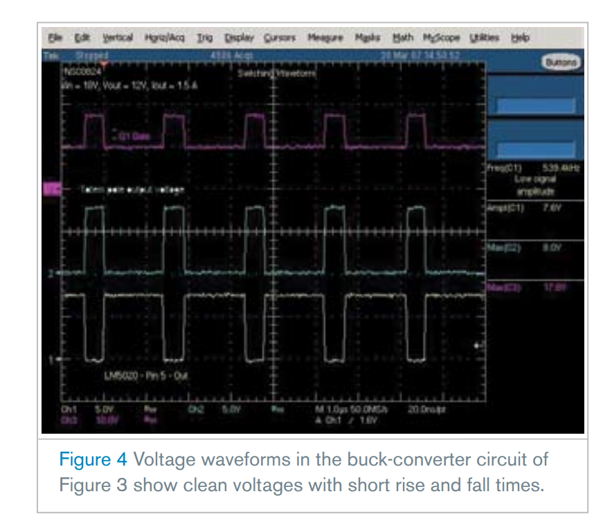
Figure 4 shows the circuit’s switching waveforms.

Oscilloscope channel 1 (bottom trace) shows the gate-drive signal that the LM5020-1 generates. Channel 2 (middle trace) shows the corresponding totem-pole output voltage. Channel 3 (top trace) shows the level-shifted totem-pole output voltage between the source and the gate of Q1. The peak value of Q1’s gate-to-source voltage equals the input voltage, and its amplitude is about 8V, the value of the supply signal that the LM5020-1 internally generates. All the waveforms are clean and have short rise and fall times. The full-load efficiency of the circuit is 86 and 83% at input voltages of 18 and 45V, respectively.