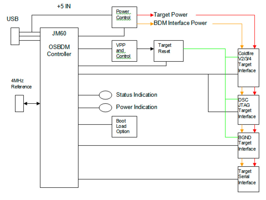


OSBDM-JM60 - 9S08JM60 Based OSBDM — It includes interfaces and firmware applied to all the targets supported by the previous open source BDMs.
It includes new features and JTAG operations. It provides interface to 9S08, 9RS08, Coldfire V1, V2, V3 and V4 target devices.
It also includes JTAG connections for DSP56800E.
OSBDM-JM60 Features
The open source BDM is implemented with the following features:
• USB 2.0 compliant communication port with standard B or mini B type connector
• The target power is determined by the MCU when OSBDM is included on a target board. Target power option of 5V or 3.3V output.
Power limited to USB requirements. Adjustable voltage output optional. Embedded OSBDM does not have the target power option
• Coldfire V2, V3, and V4 interface with port options
• BGND interface with options to support 9S08, 9RS08, and Coldfire V1 targets
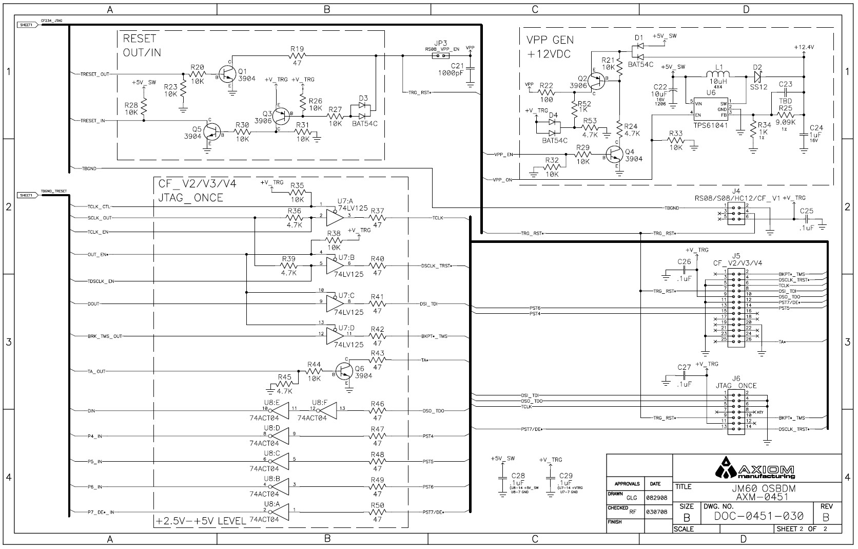
• JTAG interface to support DSC targets and JTAG option operation on Coldfire V2,V3, V4 targets
• +12Vpp generation provided for 9RS08 target
• Status and Target Power Indicators
• Boot load option to update firmware using USB connection
• Debug port for the JM60 BDM controller
• Low cost design, easy to embed on target boards requiring only one interface type
• Optional USB serial port application to pass target serial data to host Personal Computer (PC) with USB connection
OSBDM Development Port Interfaces
This section describes the individual development ports. Note that only one port type is applied to a target at any time.

BGND Interface
The BGND interface provides the standard 6 pin connection for the single wire BGND signal type development port.
Target types that apply this development port are the 9S08, RS08, and Coldfire V1.
+V_TRG, TBGND, TRG_RST*, and Ground are applied by this port type.
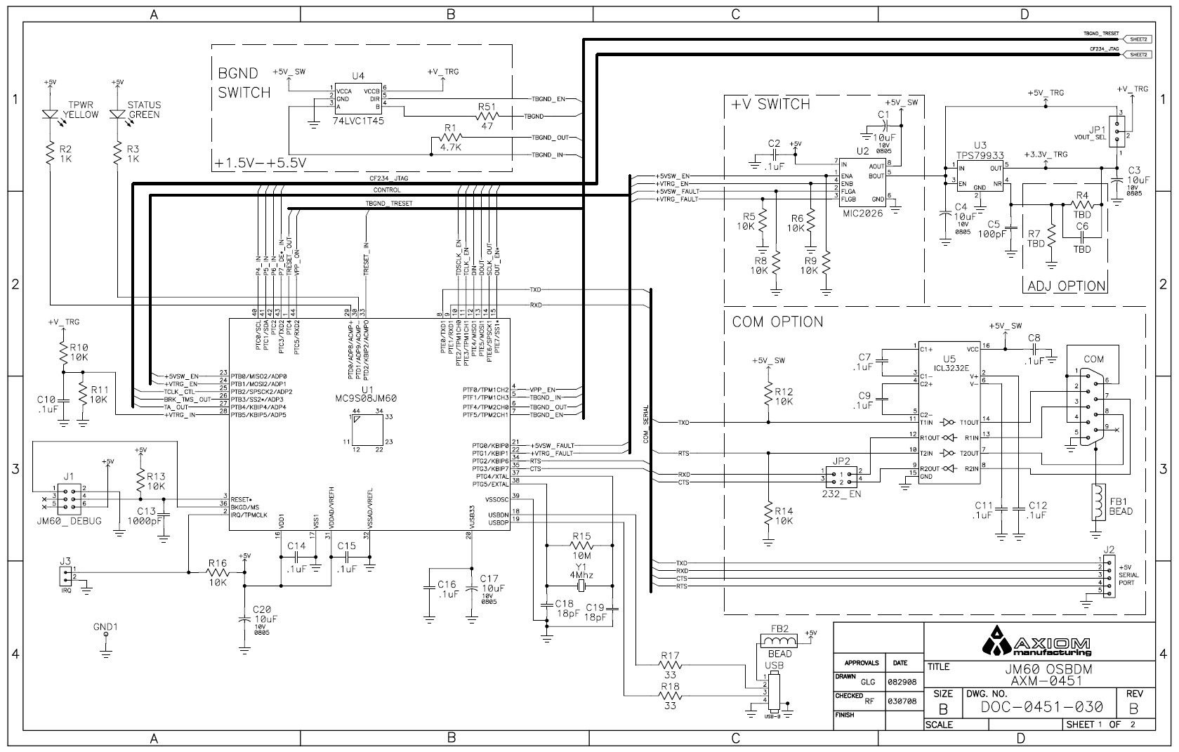
The BGND interface applies U4 as the signal transceiver.
U4 is a 74LVC1T45 logic gate with voltage level shifting features.
Operation on the target side (+V_TRG) is 1.8V to 5.5V.
The JM60 side is always +5V from the +5V_SW signal.
JM60 signals TBGND_EN, TBGND_IN, and TBGND_OUT provide the communication and control for this interface.
All these signals are associated with JM60 timer channels for precise timing capability to a 41.67ns time step period.
For more information on the input and output ports, refer to the Signal Chart section.
TBGND_ EN provides directional control for transmit or receive operations.
The signal is logic high for transmit output and logic low to receive input.
JM60 timer 2 channel 1 provides the primary signal direction control during the communication with the target.
The idle condition is low so that the interface is not driven unless the communication is intended.
During the communication, the direction is fixed to output the command to the target.
During the reception, the signal is timed in edge aligned PWM mode to provide the BGND start pulse prior to the target reply input.
TBGND_OUT provides the transmit signal output from the JM60 to the target.
Timer 2 channel 0 controls this signal in edge aligned PWM mode.
For data transmission, the timer channel will output an active low signal with a time period that represents a logic one bit value or logic 0 bit value.
In receive mode, the timer channel will provide a low output for the start bit on the BGND signal and then provide timing internally for the reply signal input time window.
TBGND_IN provides receive signal input from the target to the JM60.
Timer 1 channel 3 is applied to measure the input signal duration in capture mode (25Mhz BDC clock maximum).
This operation provides the timing to determine a logic 1 or 0 bit value input from the target.
RS08 type targets apply a lower speed communication technique that inputs the JM60 port value (sample mode) instead of using the timer capture.
This is due to the RS08 will not provide a stable input signal after the start bit generation and creates false timer capture edges.
Other undefined target types may exhibit the same issue and may apply sample mode, if required (10MHz BDC clock maximum).
NOTE The TBGND_OUT and TBGND_IN signals are connected with resistor R1. R1 provides isolation between the 2 timer channels.