http://www.st.com/web/en/resource/technical/document/application_note/CD00164185.pdf AN2586
The device requires a 2.0 V to 3.6 V operating voltage supply (VDD).
An embedded regulator is used to supply the internal 1.8 V digital power.
The real-time clock (RTC) and backup registers can be powered from the VBAT voltage
when the main VDD supply is powered off.
VDDA and VSSA must be connected to VDD and VSS, respectively

Independent A/D converter supply and reference voltage
To improve conversion accuracy, the ADC has an independent power supply that can be
filtered separately, and shielded from noise on the PCB.
● the ADC voltage supply input is available on a separate VDDA pin
● an isolated supply ground connection is provided on the VSSA pin
When available (depending on package), VREF– must be tied to VSSA.
On 100-pin and 144-pin packages
To ensure a better accuracy on low-voltage inputs, the user can connect a separate external
reference voltage ADC input on VREF+. The voltage on VREF+ may range from 2.4 V to VDDA.
On packages with 64 pins or less
The VREF+ and VREF- pins are not available, they are internally connected
to the ADC voltage supply (VDDA) and ground (VSSA).
Battery backup
To retain the content of the Backup registers when VDD is turned off, the VBAT pin can be
connected to an optional standby voltage supplied by a battery or another source.
The VBAT pin also powers the RTC unit, allowing the RTC to operate even when the main
digital supply (VDD) is turned off. The switch to the VBAT supply is controlled by the power
down reset (PDR) circuitry embedded in the Reset block.
If no external battery is used in the application, it is highly recommended to connect VBAT
externally to VDD.
Power supply schemes
The circuit is powered by a stabilized power supply, VDD.
● Caution:
– If the ADC is used, the VDD range is limited to 2.4 V to 3.6 V
– If the ADC is not used, the VDD range is 2.0 V to 3.6 V
● The VDD pins must be connected to VDD with external decoupling capacitors
(one 100 nF Ceramic capacitor for each VDD pin + one Tantalum or Ceramic capacitor
(min. 4.7 µF typ.10 µF).
● The VBAT pin can be connected to the external battery (1.8 V < VBAT < 3.6 V).
If no external battery is used, it is recommended to connect this pin to VDD
with a 100 nF external ceramic decoupling capacitor.
● The VDDA pin must be connected to two external decoupling capacitors
(100 nF Ceramic + 1 µF Tantalum or Ceramic).
● The VREF+ pin can be connected to the VDDA external power supply.
If a separate, external reference voltage is applied on VREF+,
a 100 nF and a 1 µF capacitors must be connected on this pin.
In all cases, VREF+ must be kept between 2.4 V and VDDA.
● Additional precautions can be taken to filter analog noise:
– VDDA can be connected to VDD through a ferrite bead.
– The VREF+ pin can be connected to VDDA through a resistor (typ. 47 Ω).

The STM32F1xx does not require an external reset circuit to power-up correctly.
Only a pulldown capacitor is recommended to improve EMS performance by protecting the device against parasitic resets.
Charging and discharging a pull-down capacitor through an internal resistor increases the device power consumption.
The capacitor recommended value (100 nF) can be reduced to 10 nF to limit this power consumption;

Clocks
Three different clock sources can be used to drive the system clock (SYSCLK):
● HSI oscillator clock (high-speed internal clock signal)
● HSE oscillator clock (high-speed external clock signal)
● PLL clock
The devices have two secondary clock sources:
● 40 kHz low-speed internal RC (LSI RC) that drives the independent watchdog and,
optionally, the RTC used for Auto-wakeup from the Stop/Standby modes.
● 32.768 kHz low-speed external crystal (LSE crystal) that optionally drives the real-time clock (RTCCLK)
Each clock source can be switched on or off independently when it is not used, to optimize the power consumption.


Boot mode selection

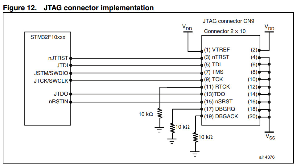
Debug management