https://flashdba.com/2014/06/20/understanding-flash-blocks-pages-and-program-erases/
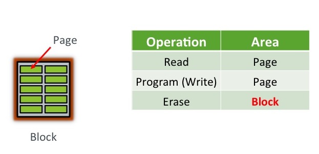
In the last post on this subject I described the invention of NAND flash and the way in which erase operations affect larger areas than write operations. Let’s have a look at this in more detail and see what actually happens. First of all, we need to know our way around the different entities on a flash chip (or “package“), which are: the die, the plane, the block and the page:
Note: What follows is a high-level description of the generic behaviour of flash. There are thousands of different NAND chips available, each potentially with slightly different instruction sets, block/page sizes, performance characteristics etc.
- The package is the memory chip, i.e. the black rectangle with little electrical connectors sticking out of it. If you look at an SSD, a flash card or the internals of a flash array you will see many flash packages, each of which is produced by one of the big flash manufacturers: Toshiba, Samsung, Micron, Intel, SanDisk, SK Hynix. These are the only companies with the multi-billion dollar fabrication plants necessary to make NAND flash.
- Each package contains one or more dies (for example one, two, or four). The die is the smallest unit that can independently execute commands or report status.
- Each die contains one or more planes (usually one or two). Identical, concurrent operations can take place on each plane, although with some restrictions.
- Each plane contains a number of blocks, which are the smallest unit that can be erased. Remember that, it’s really important.
- Each block contains a number of pages, which are the smallest unit that can be programmed (i.e. written to).
The important bit here is that program operations (i.e. writes) take place to a page, which might typically be 8-16KB in size, while erase operations take place to a block, which might be 4-8MB in size. Since a block needs to be erased before it can be programmed again (*sort of, I’m generalising to make this easier), all of the pages in a block need to be candidates for erasure before this can happen.
Program / Erase Cycles
When your flash device arrives fresh from the vendor, all of the pages are “empty”. The first thing you will want to do, I’m sure, is write some data to them – which in the world of memory chips we call a program operation. As discussed, these program operations take place at the page level. You can then read your fresh data back out again with readoperations, which also take place at the page level. [Having said that, the instruction to read a page places the data from that page in a memory register, so your reading process can in fact then selectively access subsets of the page if it desires – but maybe that’s going into too much detail…]
 Where it gets interesting is if you want to update the data you just wrote. There is no update operation for flash, no undo or rewind mechanism for changing what is currently in place, just the erase operation. It’s a little bit like an etch-a-sketch, in that you can continue to turn the dials and make white sections of screen go black, but you cannot turn black sections of screen to white again without erasing the entire screen.
  An erase operation on a flash chip clears the data from all pages in the block, so if some of the other pages contain active data (stuff you want to keep) you either have to copy it elsewhere first or hold off from doing the erase.
In fact, that second option (don’t erase just yet) makes the most sense, because the blocks on a flash chip can only tolerate a limited number of program and erase options (known as the program erase cycle or PE cycle because for obvious reasons they follow each other in turn). If you were to erase the block every time you wanted to change the contents of a page, your flash would wear out very quickly.
So a far better alternative is to simply mark the old page (containing the unchanged data) as INVALID and then write the new, changed data to an empty page. All that is required now is a mechanism for pointing any subsequent access operations to the new page and a way of tracking invalid pages so that, at some point, they can be “recycled”.

Updating a page in NAND flash. Note that the new page location does not need to be within the same block, or even the same flash die. It is shown in the same block here purely for ease of drawing.
This “mechanism” is known as the flash translation layer and it has responsibility for these tasks as well as a number of others. We’ll come back to it in subsequent posts because it is a real differentiator between flash products. For now though, think about the way the device is filling up with data. Although we’ve delayed issuing erase operations by cleverly moving data to different pages, at some point clearly there will be no empty pages left and erases will become essential. This is where the bad news comes in: it takes many times longer to perform an erase than it does to perform a read or program. And that clearly has consequences for performance if not managed correctly.
In the next post we’ll look at the differences in time taken to perform reads, programs and erases – which first requires looking at the different types of flash available: SLC, MLC and TLC…
